-
 SPICE Model
Baseband Modeling
• BSIMProPlus
RF Modeling
• MeQLab
Model Extraction Automation
• SDEP
Model QA
• ME-Pro
-
 PDK
PDKPCell Development
• PCellLab
PDK Verification
• PQLab
-
 Standard Cell
Library Characterization
• NanoCell
Library Validation
• LibWiz
-
 Fabrication
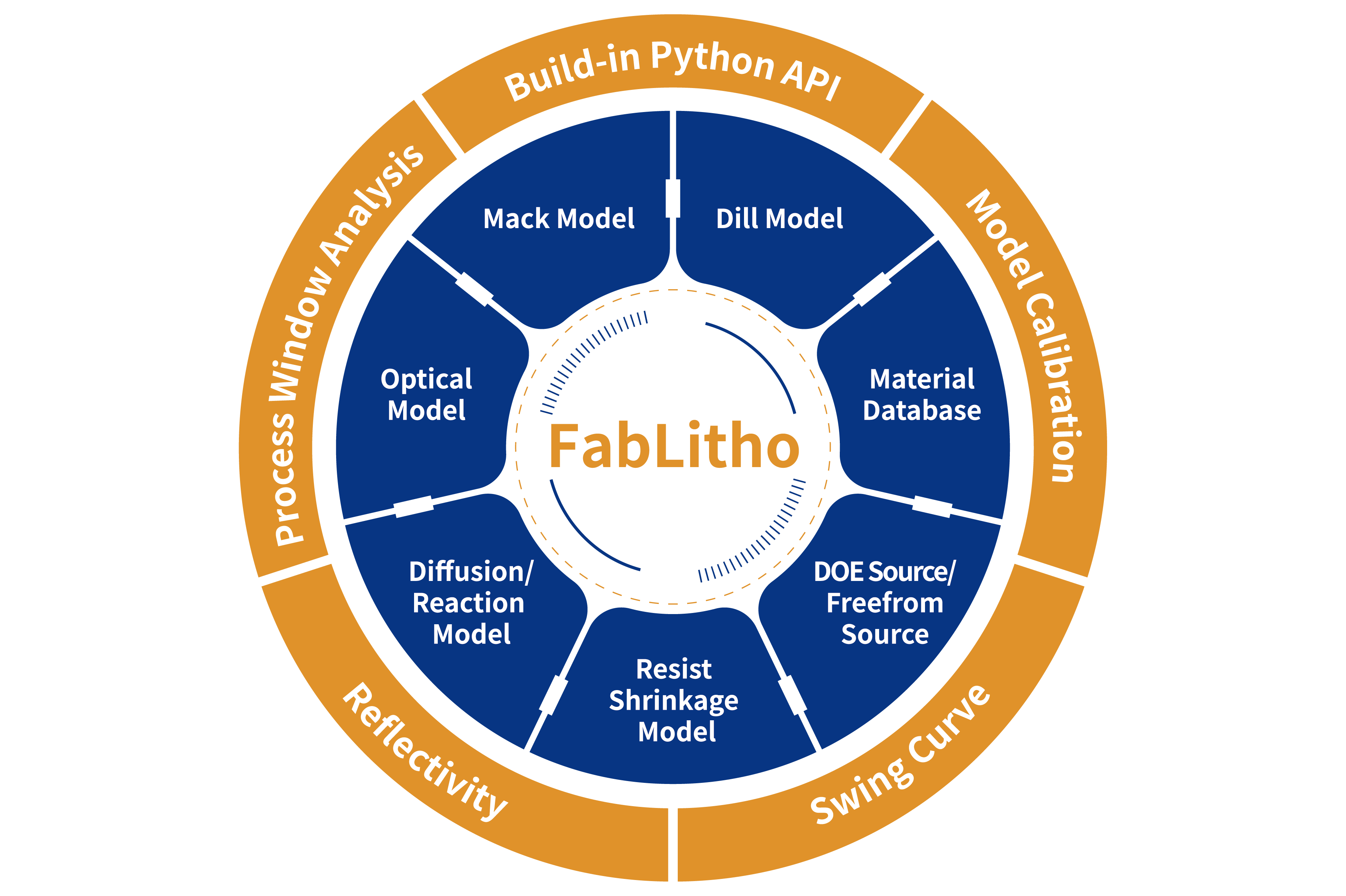
Lithography Modeling and Simulation
• FabLitho
Reticle Automated Design
• FAR
-
 Design Environment
Schematic Capture
• NanoDesigner SE
Layout Editor
• NanoDesigner LS
Interactive Physical Verification
• NanoDesigner iV
Design Optimization
• NanoDesigner Optimizer
-
 Circuit Simulation
SPICE Simulator
• NanoSpice • NanoSpice X • NanoSpice Giga
FastSPICE Simulator
• NanoSpice Pro • NanoSpice Pro X
Mixed Signal
• NanoSpice MS
Waveform Analysis
• NanoWave
-
Circuit Analysis
Static and Dynamic Circuit Check
• NanoSpice CCK
Yield Analysis
• NanoYield
Signal Integrity
• NanoSpice SI
Critical Path Analysis
• PathInspector
Power Device Design Verification
• PTM
Power Distribution Network Analysis
ESD Verification
• ESDi
-
 Circuit Simulation
Digital Simulation
• VeriSim
-
Standard Cell
Library Characterization
• NanoCell
Library Validation
• LibWiz
-
 Design & Verification
Timing Analysis
• TRASTA
Floor Planning
• NavisPro
Signal Integrity Analysis
• NanoSpice SI
Power Design Analysis
• PTM
ESD Verification
• ESDi
Chip-to-Package Connectivity Verification
• PadInspector
-
 Parametric Testing
Semiconductor Parametric Analyzer
• FS-Pro • FS800
-
 Noise Measurement
Low Frequency Noise
• 9812DX • 9812E • 9812HF
AC Dynamic Noise
• 9812AC
-
 Integrated Testing
Electrical Parameter Testing Software
• LabExpress